コンテンツ
1一般情報
2PIOモードでのデータ転送
2.1ハードウェア
2.2ソフトウェア
2.3結果
3DMAでのデータ転送
3.1ハードウェア
3.2ソフトウェア
3.3結果
4結論
5使用したソース
1一般
一般に、プロセッサモジュールとプログラム可能なロジック間のデータ転送は、次の2つのモードで可能です。
- PIO、GPポートが使用されます。
- DMA、HPポートが使用されます。
2PIOモードでのデータ転送
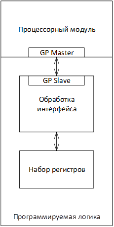
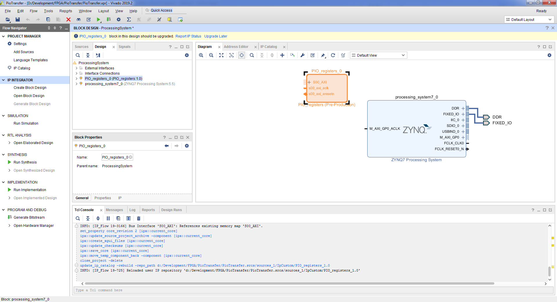
PIOモードでは、プロセッサモジュールはプログラム可能なロジックをレジスタのセットとして動作します。一定量のデータを読み書きするには、プロセッサモジュールが常に参加している必要があります。PIOモードでは、すべてのトランザクションはプロセッサモジュールによって開始されます。プログラム可能なロジックの接続には、GPポートの使用が含まれます。ここで、マスターはプロセッサモジュールであり、スレーブはプログラム可能なロジックです。 PIO使用時のプロジェクト構造
2.1ハードウェア
- チップタイプxc7z010clg400-1のVivadoでZyboのプロジェクトを作成します。
- ブロックデザインを作成します。フローナビゲーター=>ブロックデザインの作成=>名前 "ProcessingSystem" => OK。
- フィールドの「+」ボタンまたはCtrl + Iキーボードショートカットを使用して、プロセッサコアを追加します。
- [ブロック自動化の実行]ボタン=> [OK]をクリックして、必要なピンを接続しましょう。
- . Zynq7 Processing System => Import XPS Setting => => OK => OK.
- , . Tools => Create and Package New IP => Next => Create a new AXI4 peripheral => Next => , «PIO_registers» => Next => (4 ), , Lite => Next => Add IP to the repository => Finish.
- , IP . , Flow Navigator => IP Catalog.

- . Ctrl + I => PIO_registers.
- , . PIO_registers => Edit in IP Packager => OK. Vivado .
- PIO_registers_v1_0.vhd :
iSwitches : in std_logic_vector( 3 downto 0); oLeds : out std_logic_vector( 3 downto 0); ... iSwitches => iSwitches, oLeds => oLeds,
- PIO_registers_v1_0_S_AXI.vhd :
iSwitches : in std_logic_vector( 3 downto 0); oLeds : out std_logic_vector( 3 downto 0);
- :
signal SwitchesReg : std_logic_vector(31 downto 0); ... process (SwitchesReg, slv_reg1, slv_reg2, slv_reg3, axi_araddr, S_AXI_ARESETN, slv_reg_rden) variable loc_addr :std_logic_vector(OPT_MEM_ADDR_BITS downto 0); begin -- Address decoding for reading registers loc_addr := axi_araddr(ADDR_LSB + OPT_MEM_ADDR_BITS downto ADDR_LSB); case loc_addr is when b"00" => reg_data_out <= SwitchesReg; when b"01" => reg_data_out <= slv_reg1; when b"10" => reg_data_out <= slv_reg2; when b"11" => reg_data_out <= slv_reg3; when others => reg_data_out <= (others => '0'); end case; end process; process (S_AXI_ACLK) begin if (rising_edge(S_AXI_ACLK)) then if (S_AXI_ARESETN = '0') then SwitchesReg <= (others => '0'); else SwitchesReg( 3 downto 0) <= iSwitches; end if; end if; end process; process (S_AXI_ACLK) begin if (rising_edge(S_AXI_ACLK)) then if (S_AXI_ARESETN = '0') then oLeds <= (others => '0'); else oLeds <= slv_reg1( 3 downto 0); end if; end if; end process;
- vhd , Package IP – PIO_registers. . Compatibility Life Cycle Production. File Groups => Merge changes from File Group Wizard. Customization Parameters => Merge changes from Customization Parameters Wizard. Review and Package => Re-Package IP => Yes. Vivado .
- Block Design Report IP Status, Upgrade Selected => OK => Skip => OK.
- . Run Connection Automation => OK.

- block design’a. , => Make External.
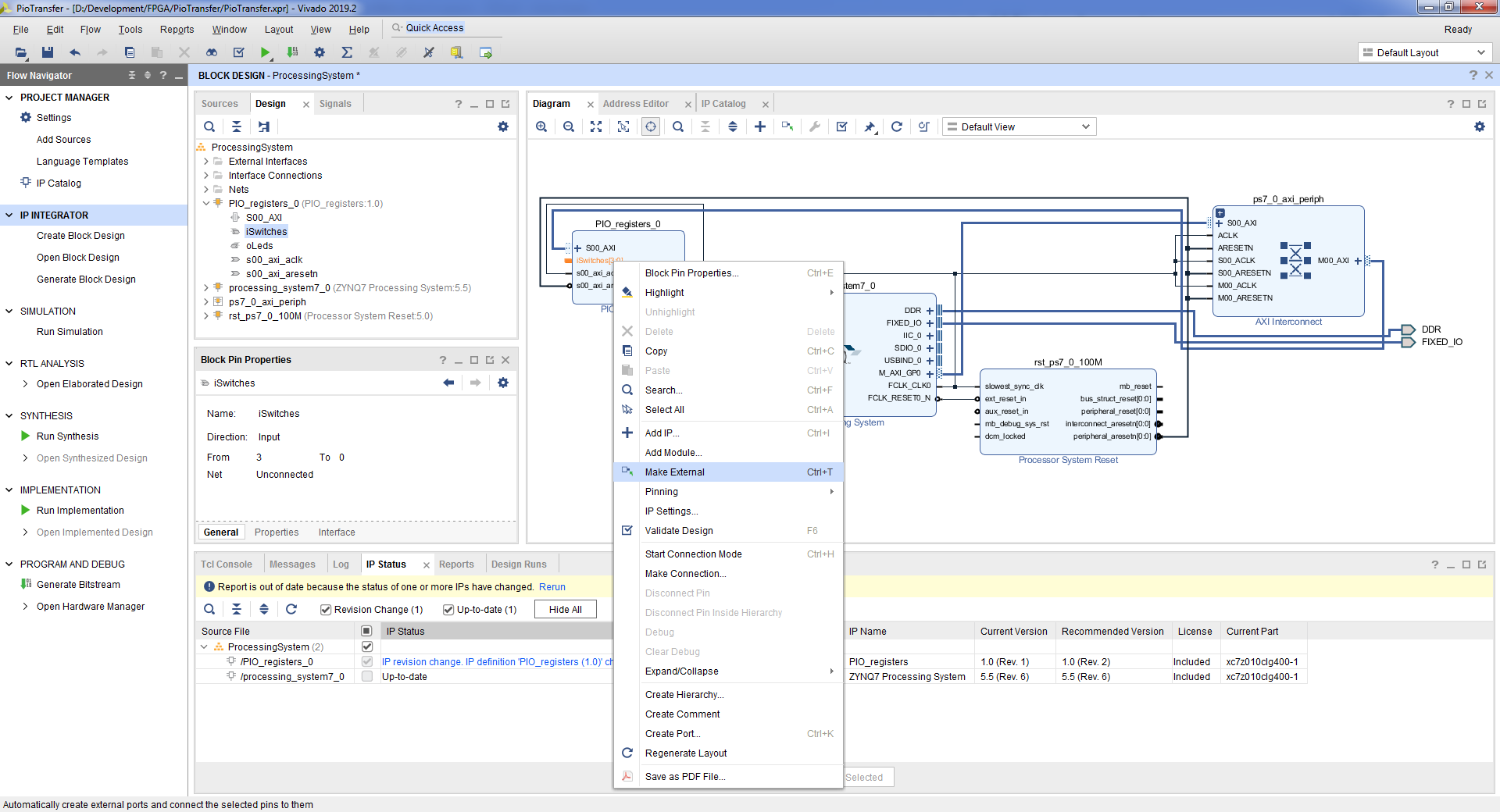
- iSwitches_0 => iSwitches. oLeds_0 => oLeds.
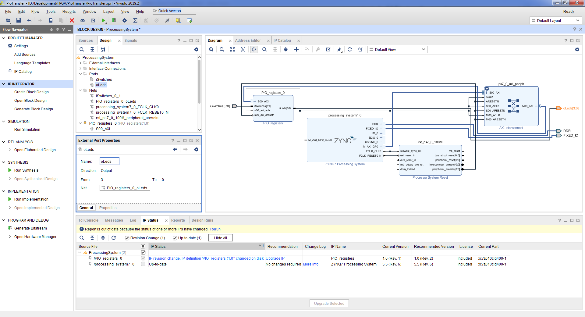
- => Tools => Validate Design => Ok.
- File => Save Block Design.
- block design , Flow Navigator => Project Manager.
- , block design’a. ProcessingSystem.bd, => View Instantiation Template.

- vhd top- block design. File => Add Sources => Add or create design sources => Next => Create File => => OK => Finish => OK => Yes.
- :
entity PioTransfer is port ( DDR_addr : inout std_logic_vector(14 downto 0 ); DDR_ba : inout std_logic_vector( 2 downto 0 ); DDR_cas_n : inout std_logic; DDR_ck_n : inout std_logic; DDR_ck_p : inout std_logic; DDR_cke : inout std_logic; DDR_cs_n : inout std_logic; DDR_dm : inout std_logic_vector( 3 downto 0 ); DDR_dq : inout std_logic_vector(31 downto 0 ); DDR_dqs_n : inout std_logic_vector( 3 downto 0 ); DDR_dqs_p : inout std_logic_vector( 3 downto 0 ); DDR_odt : inout std_logic; DDR_ras_n : inout std_logic; DDR_reset_n : inout std_logic; DDR_we_n : inout std_logic; FIXED_IO_ddr_vrn : inout std_logic; FIXED_IO_ddr_vrp : inout std_logic; FIXED_IO_mio : inout std_logic_vector( 53 downto 0 ); FIXED_IO_ps_clk : inout std_logic; FIXED_IO_ps_porb : inout std_logic; FIXED_IO_ps_srstb : inout std_logic; -- Control iSwitches : in std_logic_vector( 3 downto 0 ); oLeds : out std_logic_vector( 3 downto 0 ) ); end PioTransfer; architecture Behavioral of PioTransfer is begin PS : entity WORK.ProcessingSystem port map ( DDR_addr => DDR_addr, DDR_ba => DDR_ba, DDR_cas_n => DDR_cas_n, DDR_ck_n => DDR_ck_n, DDR_ck_p => DDR_ck_p, DDR_cke => DDR_cke, DDR_cs_n => DDR_cs_n, DDR_dm => DDR_dm, DDR_dq => DDR_dq, DDR_dqs_n => DDR_dqs_n, DDR_dqs_p => DDR_dqs_p, DDR_odt => DDR_odt, DDR_ras_n => DDR_ras_n, DDR_reset_n => DDR_reset_n, DDR_we_n => DDR_we_n, FIXED_IO_ddr_vrn => FIXED_IO_ddr_vrn, FIXED_IO_ddr_vrp => FIXED_IO_ddr_vrp, FIXED_IO_mio => FIXED_IO_mio, FIXED_IO_ps_clk => FIXED_IO_ps_clk, FIXED_IO_ps_porb => FIXED_IO_ps_porb, FIXED_IO_ps_srstb => FIXED_IO_ps_srstb, -- Control iSwitches => iSwitches, oLeds => oLeds ); end Behavioral;
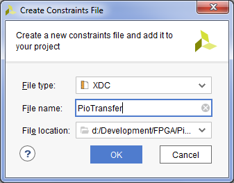
- . File => Add sources => Add or create constrains => Next => Create File => => OK => Finish.
- :
#Switches set_property PACKAGE_PIN G15 [get_ports {iSwitches[0]}] set_property PACKAGE_PIN P15 [get_ports {iSwitches[1]}] set_property PACKAGE_PIN W13 [get_ports {iSwitches[2]}] set_property PACKAGE_PIN T16 [get_ports {iSwitches[3]}] set_property IOSTANDARD LVCMOS33 [get_ports {iSwitches[*]}] #LEDs #IO_L23P_T3_35 set_property PACKAGE_PIN M14 [get_ports {oLeds[0]}] set_property PACKAGE_PIN M15 [get_ports {oLeds[1]}] set_property PACKAGE_PIN G14 [get_ports {oLeds[2]}] set_property PACKAGE_PIN D18 [get_ports {oLeds[3]}] set_property IOSTANDARD LVCMOS33 [get_ports {oLeds[*]}]
- . Flow Navigator => Generate Bitstream => OK. , , .
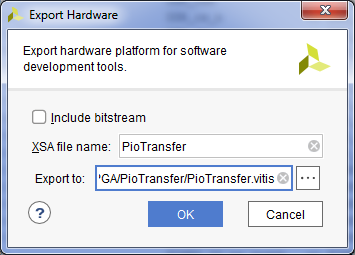
- . File => Export => Export Hardware => => OK. .xsa
2.2
次に、プログラム可能なロジックからデータを読み取り、プログラム可能なロジックにデータを書き込むプロセッサモジュール上で実行されるアプリケーションを作成する必要があります。 Vitis開発環境を開始し、Hello Worldテンプレートを使用してアプリケーションを作成する必要があります。この例は、前の記事[1]に示されています。
プロセッサモジュールからアクセスするために作成されたカーネルのアドレスは、Vivadoで表示できます。 Flow Navigator => Open Block Design => AddressEditorタブで。この場合、アドレスは0x43C0_0000です。レジスタはこのアドレスにあり、そこに属性が格納されており、スイッチはどの状態にあります。したがって、アドレス0x43C0_0004には、LEDに接続されているレジスタがあります。
Vitisで、helloworld.cファイルを開き、次のように入力します。
int main()
{
init_platform();
u32 Status = 0x00;
u32 Command = 0x00;
xil_printf("Hello World\n\r");
while (1)
{
Status = Xil_In32(0x43C00000);
xil_printf("Status %x\n\r", Status);
if (Status == 0x01 || Status == 0x02 || Status == 0x04 || Status == 0x08)
{
Command = 0x01;
}
else if (Status == 0x03 || Status == 0x5 || Status == 0x06 || Status == 0x9 || Status == 0xA || Status == 0x0C)
{
Command = 0x03;
}
else if (Status == 0x7 || Status == 0x0B || Status == 0x0D || Status == 0x0E)
{
Command = 0x7;
}
else if (Status == 0x0F)
{
Command = 0x0F;
}
else
{
Command = 0x00;
}
xil_printf("Command %x\n\r", Command);
Xil_Out32(0x43C00004, Command);
usleep(1000000);
}
cleanup_platform();
return 0;
}
ここで、Xil_In32関数を使用してプログラム可能なロジックから4バイトのデータを読み取り、Xil_Out32を使用して4バイトのデータをプログラム可能なロジックに書き込みます。
2.3結果
アプリケーションをアセンブルし、ファームウェアファイルを作成して、ボードにアップロードします。前回の記事[1]で説明されています。
起動し、com-portモニターを確認します。
Xilinx First Stage Boot Loader Release 2019.2 Dec 9 2020-15:16:52 Silicon Version 3.1 Boot mode is QSPI SUCCESSFUL_HANDOFF FSBL Status = 0x1 Hello World Status 0 Command 0 Status 8 Command 1 Status C Command 3 Status D Command 7 Status F Command F
すべてが正しく機能します。
したがって、PIOモードでプログラマブルロジックにアクセスするには、プロセッサモジュールがイニシエータであるプログラマブルロジックのプロセッサモジュールとの通信インターフェイスの1つを実装する必要があります。このインターフェイスは、GPポートによってのみ表されます。
プログラム可能なロジックへの要求がGPポートを介してどれだけ迅速に処理されるかを見てみましょう。これを行うには、プロセッサモジュールで実行されているアプリケーションで、プログラム可能なロジックのレジスタに連続して複数のエントリを追加し、デバッガにプルされたバス信号を使用してプログラム可能なロジックのトランザクション間の時間を測定します。
Axi-Liteバスが100MHzで実行されている場合、要求間の一時停止は平均23クロックサイクルです。バス周波数を200MHzに変えてみましょう。リクエスト間の一時停止は平均33サイクルになります。
合計4バイトのデータが100MHzで23クロック送信されます。速度は次のとおりです。32/(23 * 10ns)= 139 130434ビット/秒≈135869Kbps≈132Mbps≈16MB/秒。
合計4バイトのデータが200MHzで33クロック送信されます。速度は32 /(33 * 5ns)= 193939393bps≈189393Kbps≈184Mbps≈23Mbpsです。
したがって、23 MB / sの速度を達成できますが、プロセッサモジュールが常に関与します。
プロジェクト: github.com/Finnetrib/PioTransfer
3DMAモードでのデータ転送
DMAモードでのデータ転送は、プロセッサモジュールがデータ交換パラメータを設定し、交換に直接参加しないことを意味します。したがって、2つの目標が達成されます。それは、プロセッサモジュールの負荷を軽減することと、データ処理速度を向上させることです。この代償は、ハードウェアの複雑さです。
Zynqでは、DMA機能を実装する複数のipコアを使用できます。この記事では、コアAXIDMA [2]について説明します。
AXI DMAには、MM2SとS2MMの2つのチャネルがあります。チャネルMM2S(ストリームにメモリマップ)は、プロセッサモジュールからプログラム可能なロジックにデータを転送するために使用されます。 S2MM(Stream to memory-mapped)チャネルは、プログラム可能なロジックからプロセッサモジュールにデータを転送するために使用されます。チャネルは互いに独立して機能します。
AXIDMAには2つの使用例があります。
- 直接登録モード
- スキャッター/ギャザーモード
ダイレクトレジスタモードでは、1セットのレジスタを使用します。これにより、1つのバッファをプログラム可能なロジックからプロセッサモジュールに、またはその逆に転送できます。たとえば、プログラム可能なロジックからプロセッサモジュールにデータバッファを転送するには、アドレスフィールドとバッファサイズフィールドに入力して、DMAを開始する必要があります。その結果、DMAはプロセッサユニットの1つのバッファを満たし、停止します。
スキャッター/ギャザーモードは、記述子のリストを使用します。DMAは、記述子に記述されているバッファーを処理し、次の記述子に記述されているバッファーの処理に進みます。
3.1ハードウェア

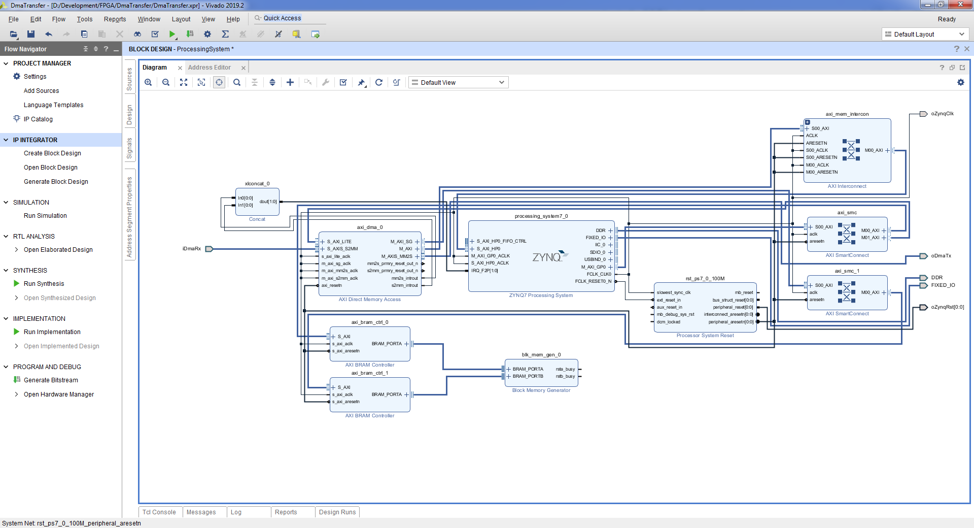
DMAを使用する場合のプロジェクト構造
記述子のリストがプログラム可能なロジックに格納されている場合のバリアントについて考えてみましょう。DMAブロックには、プロセッサユニットのGPポートに接続する制御ポートがあります。プロセッサRAMへのアクセスに使用されるHPポートもあります。記述子リストは記述子メモリに保存されます。記述子メモリには、DMAとプロセッサユニットの両方からアクセスできます。プロセッサモジュールが記述子を入力し、DMAが記述子を読み取ります。
- ブロックデザインを作成します。フローナビゲーター=>ブロックデザインの作成=>名前 "ProcessingSystem" => OK。
- フィールドの「+」ボタンまたはCtrl + Iキーボードショートカットを使用して、プロセッサコアを追加します。
- [ブロック自動化の実行]ボタン=> [OK]をクリックして、必要なピンを接続しましょう。
- . Zynq7 Processing System => Import XPS Setting => => OK => OK
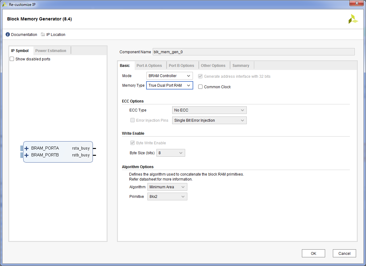
- AXI Direct Memory Access, AXI BRAM Controller, Block Memory Generator.
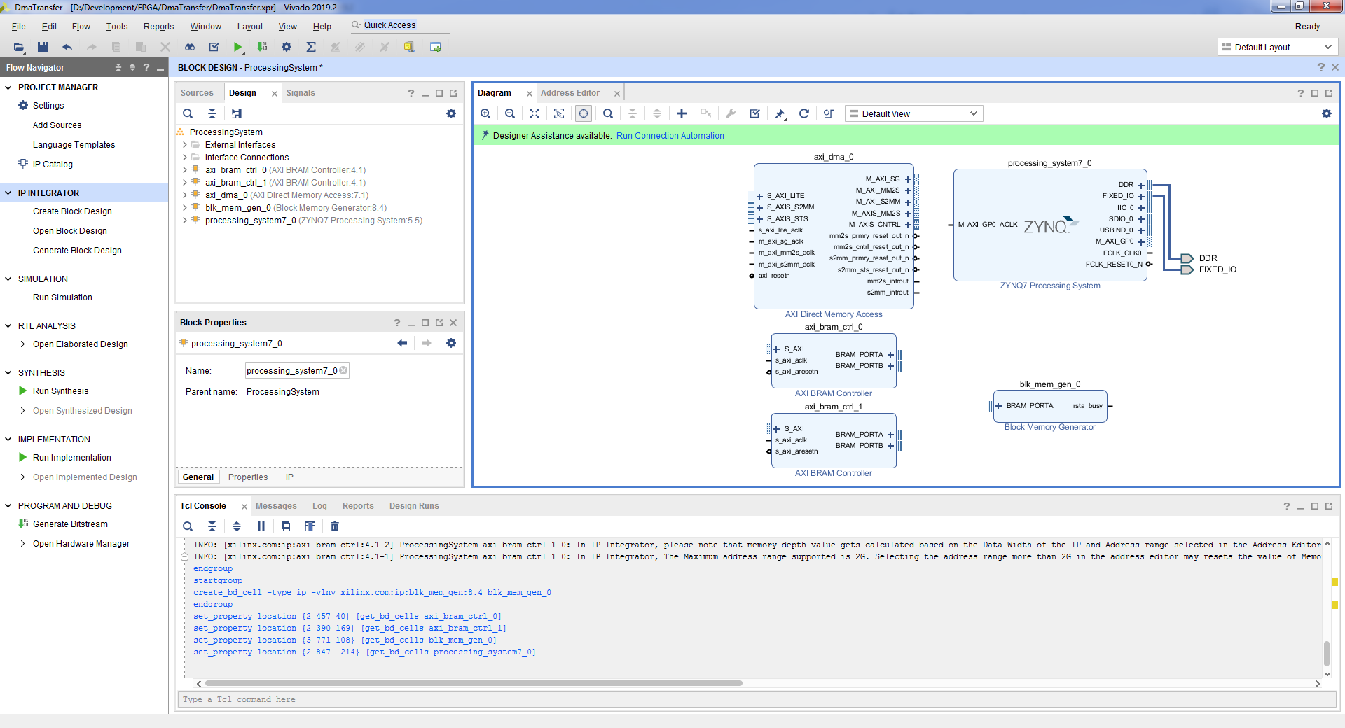
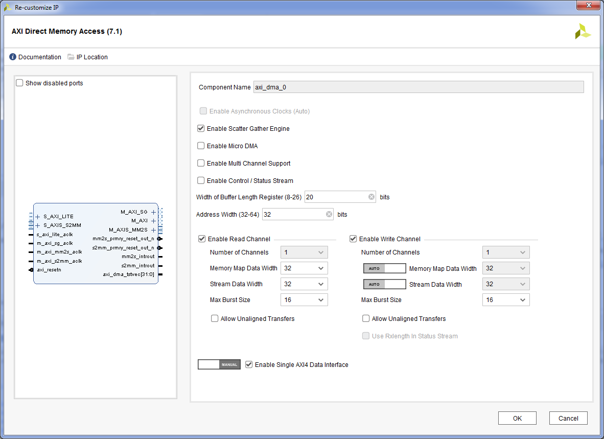
- AXI Direct Memory Access, . «Enable Scatter Gather Engine» , . «Enable Control / Status Stream» AXI Ethernet, . «With of Buffer Length Register» , . 20, 2^20 = 1 048 576 . «Address With» . 32 . «Enable Read Channel» «Enable Write Channel» . «Enable Single AXI4 Data interface» , . «OK» .
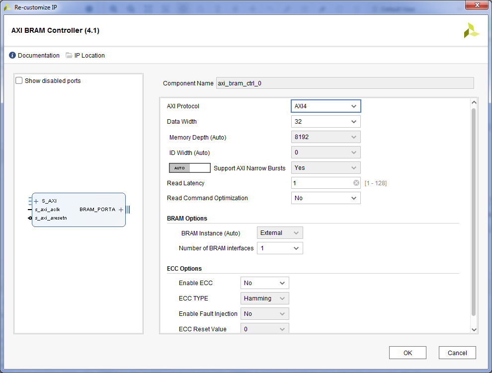
- AXI BRAM Controller. «Number of BRAM Interfaces» 1. «OK» .
- AXI BRAM Controller.
- Block Memory Generator. «Memory Type» «True Dual Port RAM». «OK» .
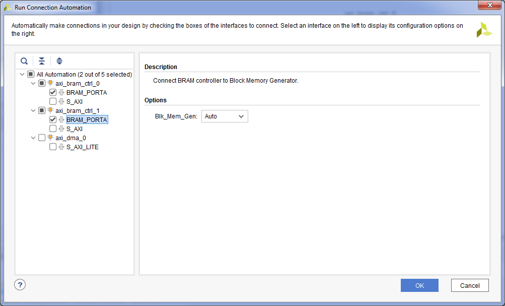
- . «Run Connection Automation» => axi_bram_ctrl_0 BRAM_PORTA => axi_bram_ctrl_1 BRAM_PORTA => OK.
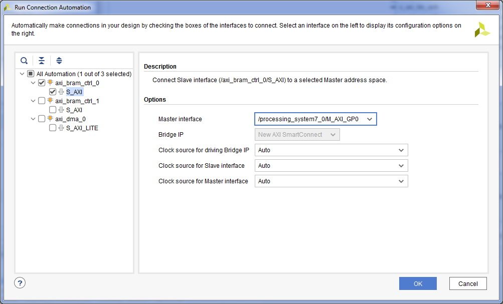
- . «Run Connection Automation» => axi_bram_ctrl_0 S_AXI => Master Interface /processing_system7_0/M_AXI_GP0 => OK. , .
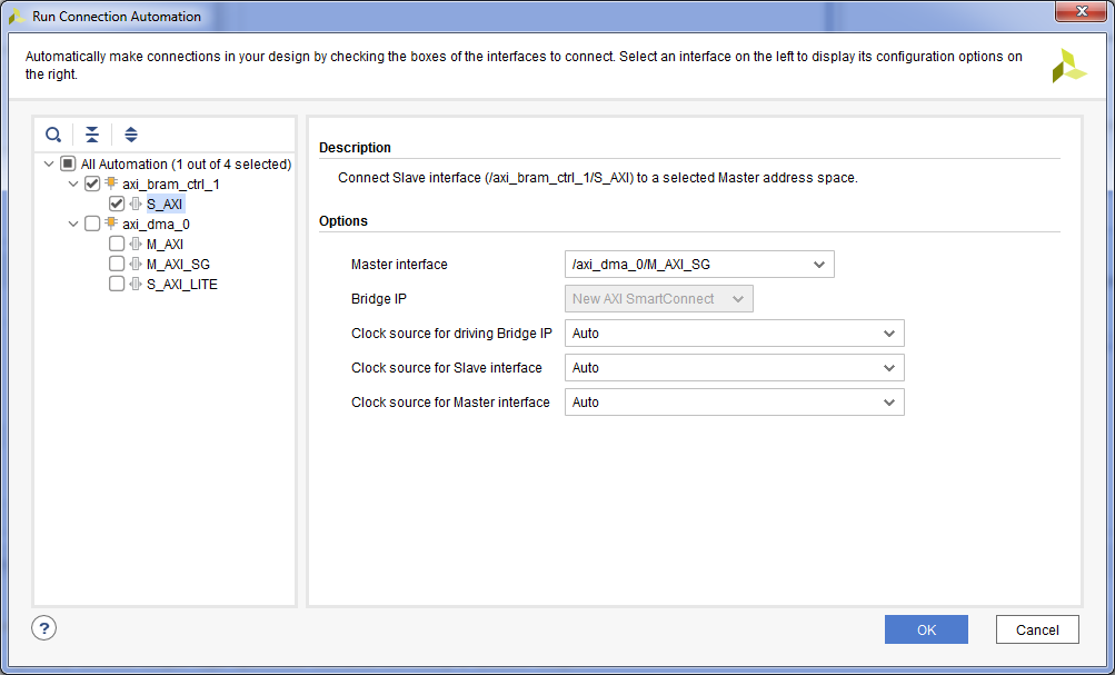
- DMA. «Run Connection Automation» => axi_bram_ctrl_1 S_AXI => Master Interface /axi_dma_0/M_AXI_SG => OK. , DMA .
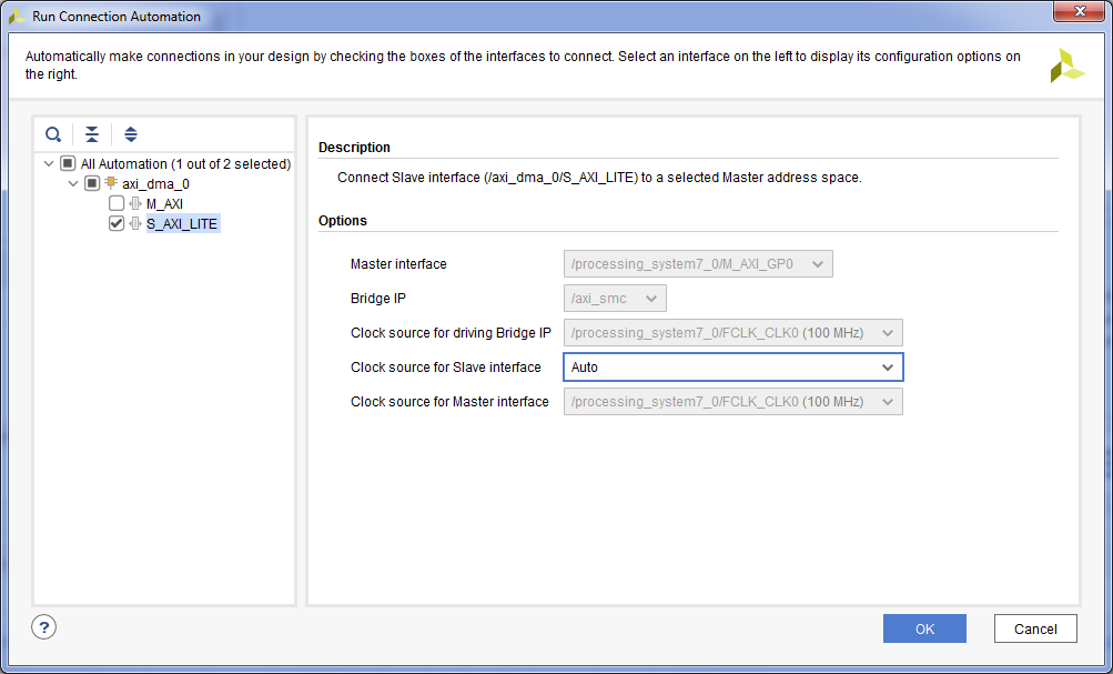
- DMA . «Run Connection Automation» => axi_dma_0 S_AXI_LITE => OK.
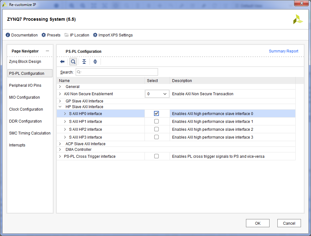
- – HP . Zynq7 Processing System => PS-PL Configuration => HP Slave AXI Interface => S AXI HP0 Interface.
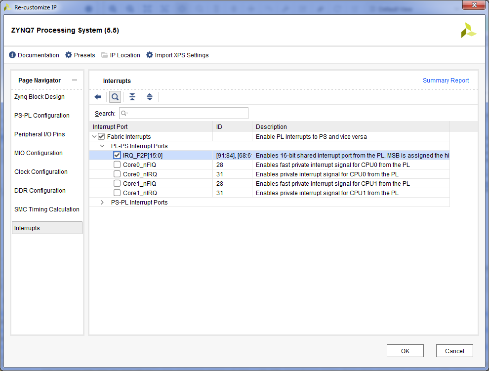
Interrupts => Fabric Interrupts => PL-PS Interrupts Ports => Fabric Interrupts => IRQ_F2P => OK.
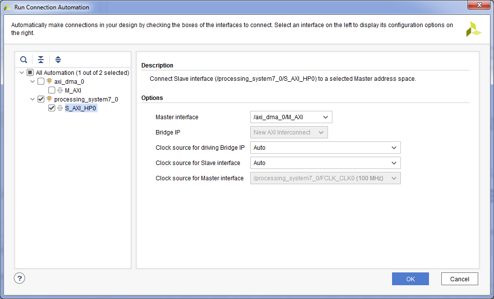
- DMA . «Run Connection Automation» => processing_system7_0 S_AXI_HP0 => Master Interface /axi_dma_0/M_AXI => OK.
- DMA . Concat + Ctrl + I.
- mm2s_introut DMA, . mm2s_introut In0 Concat. , , .
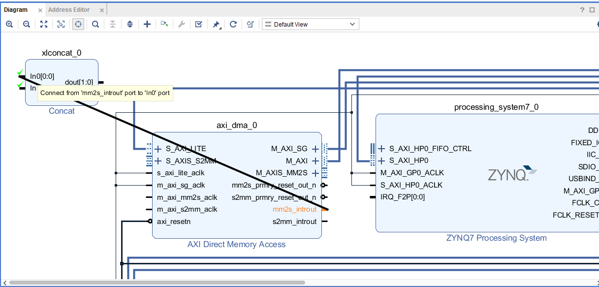
- s2mm_introut, In1 Concat.
- dout Concat IRQ_F2P Zynq7 Processing System.
- DMA . DMA . Block Design, . Create Port Ctrl + K. , => OK.
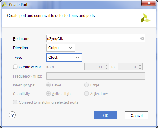
- FCLK_CLK0 Zynq7 Processing System.
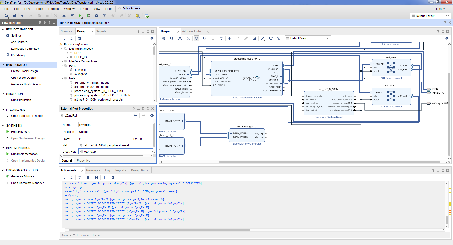
- . peripheral_reset Processor System Reset => => Make External.
- , , .
- DMA. S_AXIS_S2MM AXI Direct Memory Access => => Make External.
- , , .
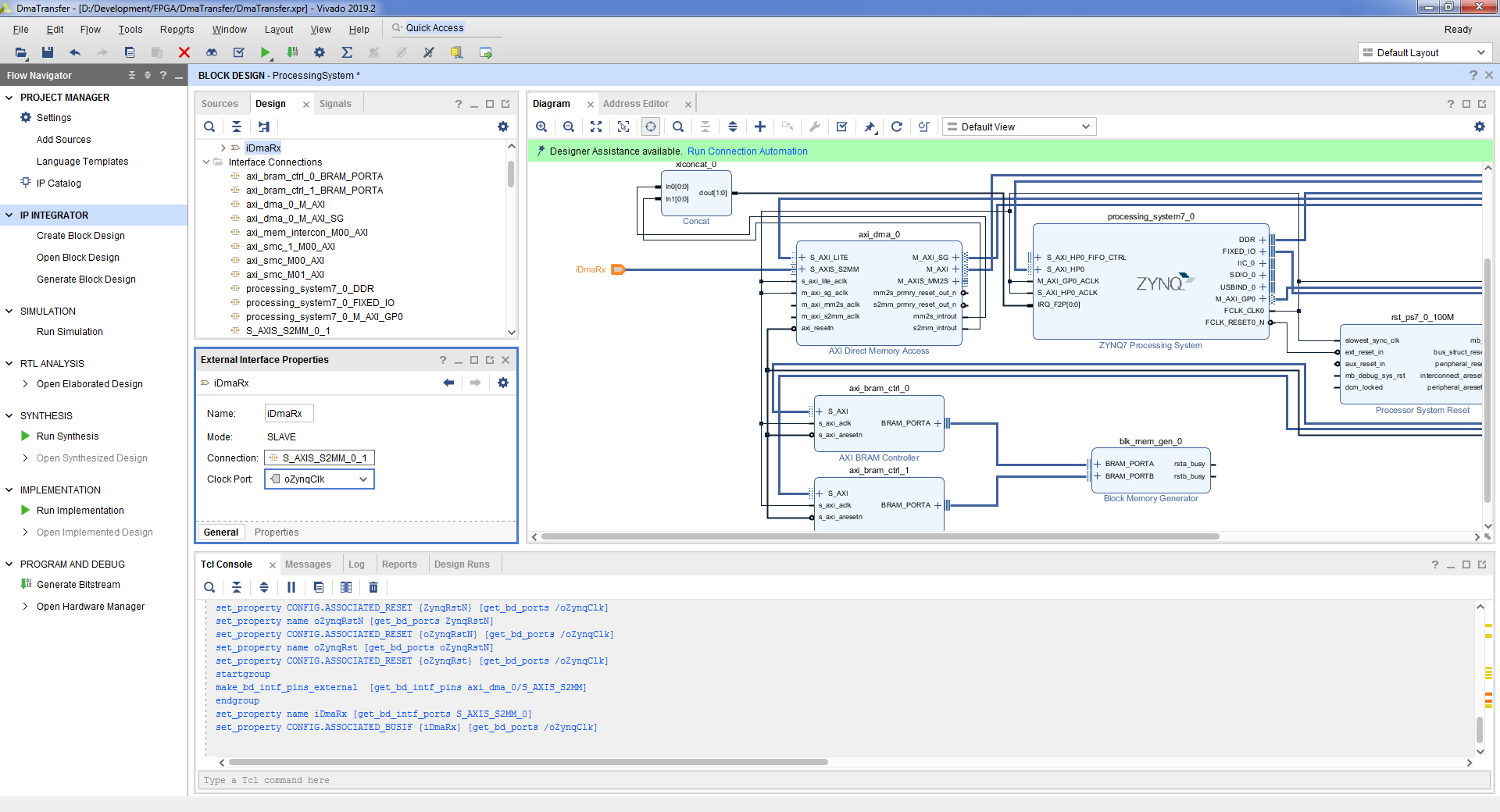
- DMA. M_AXIS_MM2S AXI Direct Memory Access => => Make External.
- , , .

- S_AXIS_S2MM M_AXIS_MM2S AXI Direct Memory Access. «Run Connection Automation» => m_axi_mm2s_aclk m_axi_s2mm_aclk => OK
- , DMA . . Address Editor => processing_system7_0 / Data / axi_bram_ctrl_0 => Offset Address 0x4000_0000 => Range 32K. axi_dma_0 / Data_SG / axi_bram_ctrl_1 => Offset Address 0x4000_0000 => Range 32K.
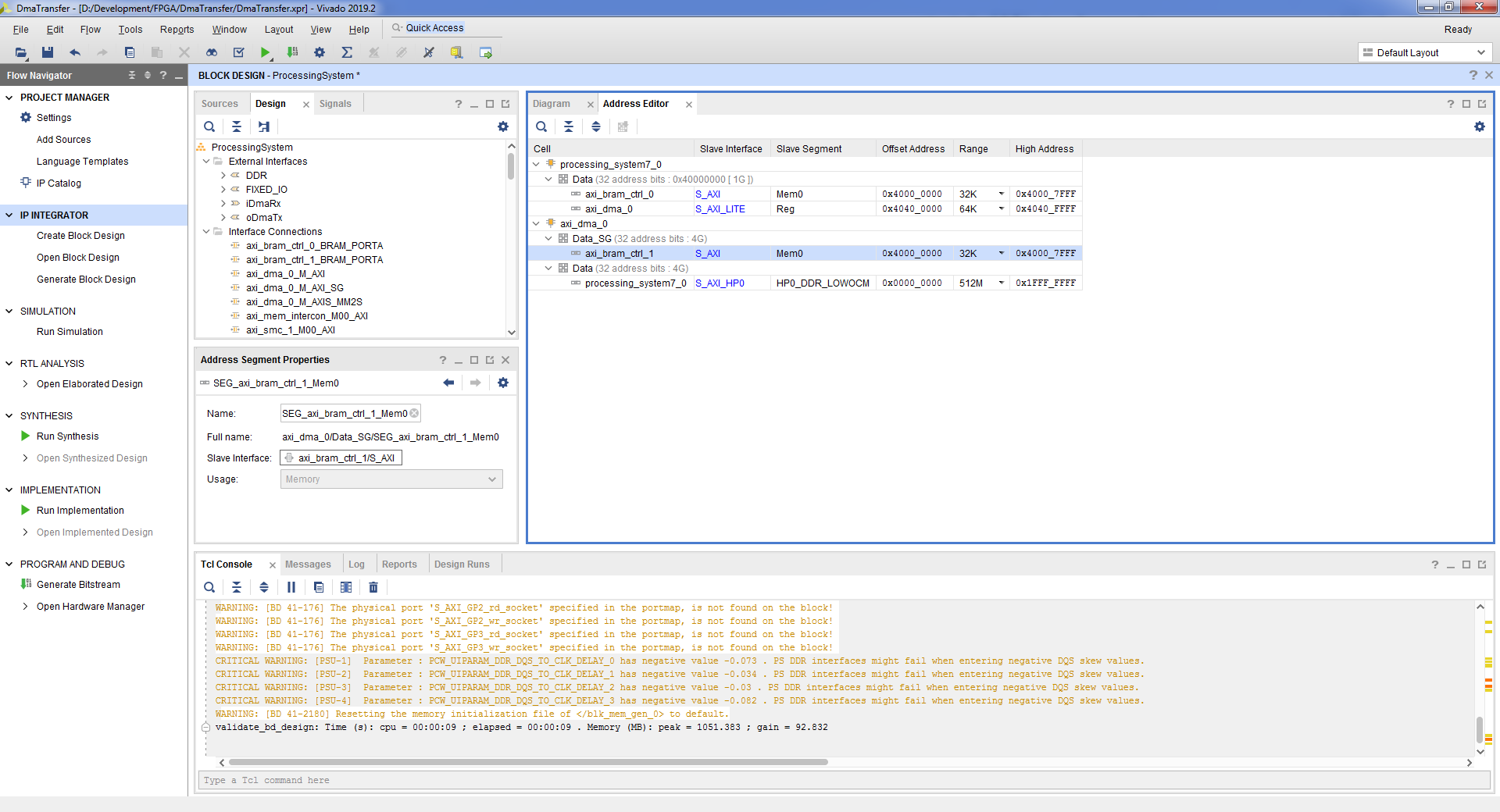
- Tools => Validate Design => OK. :
- File => Save Block Design.
- block design , Flow Navigator => Project Manager.
- , block design’a. ProcessingSystem.bd, => View Instantiation Template.
- vhd top- block design. File => Add Sources => Add or create design sources => Next => Create File => => OK => Finish => OK => Yes.

- :
entity DmaTransfer is port ( DDR_addr : inout std_logic_vector(14 downto 0); DDR_ba : inout std_logic_vector( 2 downto 0); DDR_cas_n : inout std_logic; DDR_ck_n : inout std_logic; DDR_ck_p : inout std_logic; DDR_cke : inout std_logic; DDR_cs_n : inout std_logic; DDR_dm : inout std_logic_vector( 3 downto 0); DDR_dq : inout std_logic_vector(31 downto 0); DDR_dqs_n : inout std_logic_vector( 3 downto 0); DDR_dqs_p : inout std_logic_vector( 3 downto 0); DDR_odt : inout std_logic; DDR_ras_n : inout std_logic; DDR_reset_n : inout std_logic; DDR_we_n : inout std_logic; FIXED_IO_ddr_vrn : inout std_logic; FIXED_IO_ddr_vrp : inout std_logic; FIXED_IO_mio : inout std_logic_vector(53 downto 0); FIXED_IO_ps_clk : inout std_logic; FIXED_IO_ps_porb : inout std_logic; FIXED_IO_ps_srstb : inout std_logic ); end DmaTransfer; architecture Behavioral of DmaTransfer is signal RxData : std_logic_vector(31 downto 0); signal RxKeep : std_logic_vector( 3 downto 0); signal RxLast : std_logic; signal RxValid : std_logic; signal RxReady : std_logic; signal TxData : std_logic_vector(31 downto 0); signal TxKeep : std_logic_vector( 3 downto 0); signal TxLast : std_logic; signal TxValid : std_logic; signal TxReady : std_logic; signal clk : std_logic; signal rst : std_logic; signal FifoDataW : std_logic_vector(36 downto 0); signal FifoWrite : std_logic; signal FifoRead : std_logic; signal FifoDataR : std_logic_vector(36 downto 0); signal FifoEmpty : std_logic; signal FifoFull : std_logic; begin PS : entity WORK.ProcessingSystem port map ( DDR_addr => DDR_addr, DDR_ba => DDR_ba, DDR_cas_n => DDR_cas_n, DDR_ck_n => DDR_ck_n, DDR_ck_p => DDR_ck_p, DDR_cke => DDR_cke, DDR_cs_n => DDR_cs_n, DDR_dm => DDR_dm, DDR_dq => DDR_dq, DDR_dqs_n => DDR_dqs_n, DDR_dqs_p => DDR_dqs_p, DDR_odt => DDR_odt, DDR_ras_n => DDR_ras_n, DDR_reset_n => DDR_reset_n, DDR_we_n => DDR_we_n, FIXED_IO_ddr_vrn => FIXED_IO_ddr_vrn, FIXED_IO_ddr_vrp => FIXED_IO_ddr_vrp, FIXED_IO_mio => FIXED_IO_mio, FIXED_IO_ps_clk => FIXED_IO_ps_clk, FIXED_IO_ps_porb => FIXED_IO_ps_porb, FIXED_IO_ps_srstb => FIXED_IO_ps_srstb, -- Dma Channel iDmaRx_tdata => RxData, iDmaRx_tkeep => RxKeep, iDmaRx_tlast => RxLast, iDmaRx_tready => RxReady, iDmaRx_tvalid => RxValid, oDmaTx_tdata => TxData, oDmaTx_tkeep => TxKeep, oDmaTx_tlast => TxLast, oDmaTx_tready => TxReady, oDmaTx_tvalid => TxValid, -- System oZynqClk => clk, oZynqRst(0) => rst ); FifoDataW(31 downto 0) <= not TxData; FifoDataW(35 downto 32) <= TxKeep; FifoDataW( 36) <= TxLast; FifoWrite <= TxValid and not FifoFull; TxReady <= not FifoFull; EchFifo : entity WORK.SyncFifoBram37x1024 port map ( clk => clk, srst => rst, din => FifoDataW, wr_en => FifoWrite, rd_en => FifoRead, dout => FifoDataR, full => open, empty => FifoEmpty, prog_full => FifoFull ); RxData <= FifoDataR(31 downto 0); RxKeep <= FifoDataR(35 downto 32); RxLast <= FifoDataR(36); RxValid <= not FifoEmpty; FifoRead <= RxReady; end Behavioral;
- . Flow Navigator => Generate Bitstream => OK. , , .
- . File => Export => Export Hardware => => OK. .xsa

3.2
次に、プロセッサモジュールで実行されるアプリケーションを作成する必要があります。Vitis開発環境を開始し、Hello Worldテンプレートを使用してアプリケーションを作成する必要があります。この例は、前の記事に示されています。
Axi DMAの記述子の形式は、カーネルドキュメント[2]に記載されています。記述子のサイズは52バイトですが、記述子が配置されているアドレスは64バイトに揃える必要があります。
記述子の形式について簡単に説明します。
- NXTDESC-次の記述子のアドレス。
- NXTDESC_MSB-次の記述子アドレスの上位32ビット。
- BUFFER_ADDRESS-バッファアドレス;
- BUFFER_ADDRESS_MSB-バッファアドレスの上位32ビット。
- 予約済み-使用されていません。
- 予約済み-使用されていません。
- CONTROL-バッファサイズ、パケットの開始と終了の符号を設定します。
- STATUS-受信/送信、処理済み/未処理のバイト数を示します。
- APP0-「コントロール/ステータスストリーム」チャネルを操作するために使用されます。
- APP1-「コントロール/ステータスストリーム」チャネルを操作するために使用されます。
- APP2-コントロール/ステータスストリームチャネルを操作するために使用されます。
- APP3-「コントロール/ステータスストリーム」チャネルを操作するために使用されます。
- APP4-コントロール/ステータスストリームチャネルを操作するために使用されます。
プロセッサモジュールからアクセスするためのプログラム可能なロジックのアドレスは、Vivadoで表示できます。Flow Navigator => Open Block Design => AddressEditorタブで。この場合、DMAアドレスは0x4040_0000です。記述子のメモリ領域の先頭のアドレスは0x4000_0000です。
- Vitisで、helloworld.cファイルを開き、次のライブラリを含めます
#include <xil_io.h> #include "sleep.h" #include "xil_cache.h" #include "xil_mem.h"
- , 64 . , 32 32 768 / 64 = 512 . 256 256 .
#define DESC_COUNT 256 ... /** Descriptors for receive */ struct SGDesc RxDesc[DESC_COUNT]; /** Descriptors for transmit */ struct SGDesc TxDesc[DESC_COUNT];
- , , .
/** Flush Cache */ Xil_DCacheFlush(); /** Disable Cache */ Xil_DCacheDisable();
- , .
for (u16 desc = 0; desc < DESC_COUNT; desc++) { for (u32 i = 0; i < BUFFER_SIZE; i++) { TxBuffer[desc][i] = desc + i; } }
- .
for (u16 i = 0; i < DESC_COUNT; i++) { TxDesc[i].NXTDESC = &TxDesc[i]; TxDesc[i].NXTDESC_MSB = 0x0; TxDesc[i].BUFFER_ADDRESS = &TxBuffer[i][0]; TxDesc[i].BUFFER_ADDRESS_MSB = 0x0; TxDesc[i].RESERVED0 = 0x0; TxDesc[i].RESERVED1 = 0x0; TxDesc[i].CONTROL = 0xC000000 + sizeof(TxBuffer[i]); TxDesc[i].STATUS = 0x0; TxDesc[i].APP0 = 0x0; TxDesc[i].APP1 = 0x0; TxDesc[i].APP2 = 0x0; TxDesc[i].APP3 = 0x0; TxDesc[i].APP4 = 0x0; }
- , .
DescAddr = 0x40000000; for (u16 i = 0; i < DESC_COUNT; i++) { Xil_MemCpy(DescAddr, &TxDesc[i], sizeof(TxDesc[i])); DescAddr += 0x40; }
- .
/** Write pointer to next pointer */ DescAddr = 0x40000000; for (u16 i = 0; i < DESC_COUNT - 1; i++) { Xil_Out32(DescAddr, DescAddr + 0x40); DescAddr += 0x40; } /** Write pointer for last descriptor */ Xil_Out32(DescAddr, DescAddr);
- .
/** Fill descriptor to receive */ for (u16 i = 0; i < DESC_COUNT; i++) { RxDesc[i].NXTDESC = &RxDesc[i]; RxDesc[i].NXTDESC_MSB = 0x0; RxDesc[i].BUFFER_ADDRESS = &RxBuffer[i][0]; RxDesc[i].BUFFER_ADDRESS_MSB = 0x0; RxDesc[i].RESERVED0 = 0x0; RxDesc[i].RESERVED1 = 0x0; RxDesc[i].CONTROL = sizeof(RxBuffer[i]); RxDesc[i].STATUS = 0x0; RxDesc[i].APP0 = 0x0; RxDesc[i].APP1 = 0x0; RxDesc[i].APP2 = 0x0; RxDesc[i].APP3 = 0x0; RxDesc[i].APP4 = 0x0; } /** Copy receive descriptor for memory of descriptors */ DescAddr = 0x40000000 + 0x4000; for (u16 i = 0; i < DESC_COUNT; i++) { Xil_MemCpy(DescAddr, &RxDesc[i], sizeof(RxDesc[i])); DescAddr += 0x40; } /** Write pointer to next pointer */ DescAddr = 0x40000000 + 0x4000; for (u16 i = 0; i < DESC_COUNT - 1; i++) { Xil_Out32(DescAddr, DescAddr + 0x40); DescAddr += 0x40; } /** Write pointer for last descriptor */ Xil_Out32(DescAddr, DescAddr);
- DMA . DMA .
/** Reset DMA and setup */ /** MM2S */ Xil_Out32(0x40400000, 0x0001dfe6); Xil_Out32(0x40400000, 0x0001dfe2); /** S2MM */ Xil_Out32(0x40400030, 0x0001dfe6); Xil_Out32(0x40400030, 0x0001dfe2); /** PL => PS */ Xil_Out32(0x4040003c, 0x00000000); Xil_Out32(0x40400038, 0x40004000); Xil_Out32(0x40400030, 0x0001dfe3); Xil_Out32(0x40400044, 0x00000000); Xil_Out32(0x40400040, 0x40007FC0); /** PS => PL */ Xil_Out32(0x4040000C, 0x00000000); Xil_Out32(0x40400008, 0x40000000); Xil_Out32(0x40400000, 0x0001dfe3); Xil_Out32(0x40400014, 0x00000000); Xil_Out32(0x40400010, 0x40003FC0);
- , . , , .
/** Wait ready in last descriptor */ while (1) { status = Xil_In32(0x40003FDC); if ((status & 0x80000000) == 0x80000000) { break; } else { countWait++; usleep(100); } } xil_printf("Time %x \n\r", countWait);
3.3
アプリケーションをアセンブルし、ファームウェアファイルを作成して、ボードにアップロードします。前回の記事[1]で説明されています。
起動し、com-portモニターを確認します。
Xilinx First Stage Boot Loader Release 2019.2 Dec 16 2020-15:11:44 Silicon Version 3.1 Boot mode is QSPI SUCCESSFUL_HANDOFF FSBL Status = 0x1 Hello World Time 10F
したがって、プロセッサモジュールとプログラム可能なロジックの間でデータを交換するには、プロセッサモジュールとの通信インターフェイスの1つをプログラム可能なロジックに実装する必要があります。ここで、イニシエータはプログラム可能なロジックです。このようなインターフェイスは、ポートGP、HP、ACPで表されます。前回の記事[1]では、それらはすべて考慮されていました。
データ転送速度を計算してみましょう:(256回* 102400バイト)/(271 *100μs)≈967321033バイト/s≈944649KB/s≈922MB/ s。
ビットレート7,738,568,264bps。
理論速度は32ビット* 250 MHz = 8,000,000,000ビット/秒です。
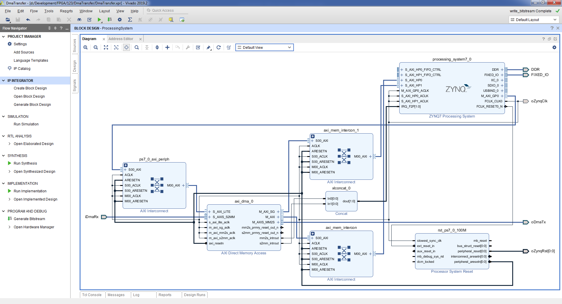
また、記述子をプログラマブルロジックメモリではなく、プロセッサモジュールに接続されたRAMに格納することもできます。この場合、M_AXI_SGポートはHPZynqポートに接続します。
データおよびプロセッサのRAM内の記述子へのDMAアクセスに異なるHPポートが使用される場合の最初のオプションを考えてみましょう。プログラム可能なロジックのファームウェアを変更して、次のスキームを取得しましょう。 異なるポートを介したデータと記述子へのアクセスアプリケーションのソースコードは提供しません。唯一の違いは、記述子をプログラム可能なロジックメモリにコピーする必要がないことです。ただし、各記述子のアドレスが64バイトにアラインされているという条件を考慮する必要があります。
アプリケーションを起動した後、com-portモニターで、データバッファーをコピーするための実行時間が変更されていないことがわかります。これも271 *100μsです。
同じポートを使用してプロセッサのRAM内のDMAと記述子にアクセスする場合は、2番目のオプションを検討してください。プログラム可能なロジックのファームウェアを変更して、次のスキームを取得しましょう。 同じポートを介したデータと記述子へのアクセスアプリケーションのソースコードは、以前のバージョンと比較して変更されていません。 アプリケーションを起動した後、com-portモニターに、バッファーコピー操作の新しい実行時間が表示されます:398 *100μs。

その結果、処理速度は(256回* 102400バイト)/(398 *100μs)≈658653266バイト/s≈643216KB/s≈628MB/ sになります。
ビットレート5269226128ビット/秒。
プロジェクト: github.com/Finnetrib/DmaTransfer
4結論
この記事では、プロセッサモジュールとプログラマブルロジック間のデータ交換の2つの実装について説明しました。PIOモードは実装が簡単で、最大23 MB / sの速度を得ることができます。DMAモードはやや複雑ですが、速度も高く、最大628 MB / sです。